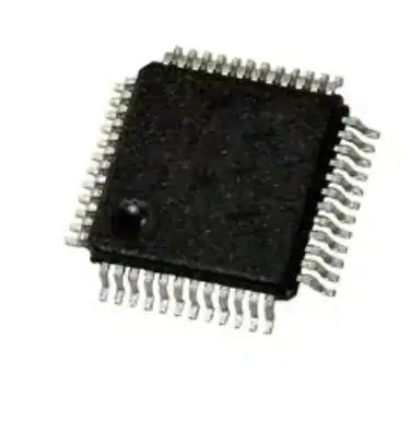
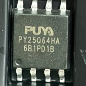
R5F100GEAFB is a high-performance, low-power 16-bit microcontroller (MCU) belonging to the RL78/G13 series manufactured by Renesas Electronics Corporation.
True low-power platform (66 μA/MHz, and 0.57 μA for operation with only RTC and LVD) for the general-purpose applications, with 1.6-V to 5.5-V operation, 16- to 512-Kbyte code flash memory, and 41 DMIPS at 32 MHz
R5F100GEAFB RENESAS MICROCONTROLLER
1.1 Features
Ultra-low power consumption technology
VDD = single power supply voltage of 1.6 to 5.5 V
HALT mode
STOP mode
SNOOZE mode
RL78 CPU core
CISC architecture with 3-stage pipeline
Minimum instruction execution time: Can be changed from high speed (0.03125 μs: @ 32 MHz operation with high-speed on-chip oscillator) to ultra-low speed (30.5 μs: @ 32.768 kHz operation with subsystem clock)
Address space: 1 MB
General-purpose registers: (8-bit register × 8) × 4 banks
On-chip RAM: 2 to 32 KB
Code flash memory
Code flash memory: 16 to 512 KB
Block size: 1 KB
Prohibition of block erase and rewriting (security function)
On-chip debug function
Self-programming (with boot swap function/flash shield window function)
Data Flash Memory
Data flash memory: 4 KB to 8 KB
Back ground operation (BGO): Instructions can be executed from the program memory while rewriting the data flash memory.
Number of rewrites: 1,000,000 times (TYP.)
Voltage of rewrites: VDD = 1.8 to 5.5 V High-speed on-chip oscillator
Select from 32 MHz, 24 MHz, 16 MHz, 12 MHz, 8 MHz,
6 MHz, 4 MHz, 3 MHz, 2 MHz, and 1 MHz
High accuracy: +/- 1.0 % (VDD = 1.8 to 5.5 V, TA = -20 to +85°C)
Operating ambient temperature
TA = -40 to +85°C (A: Consumer applications, D: Industrial applications )
TA = -40 to +105°C (G: Industrial applications) Power management and reset function
On-chip power-on-reset (POR) circuit
On-chip voltage detector (LVD) (Select interrupt and reset from 14 levels) DMA (Direct Memory Access) controller
2/4 channels
Number of clocks during transfer between 8/16-bit SFR and internal RAM: 2 clocks
Multiplier and divider/multiply-accumulator
16 bits × 16 bits = 32 bits (Unsigned or signed)
32 bits ÷ 32 bits = 32 bits (Unsigned)
16 bits × 16 bits + 32 bits = 32 bits (Unsigned or signed) Serial interface
Simplified SPI (CSI Note 1): 2 to 8 channels
UART/UART (LIN-bus supported): 2 to 4 channels
I2C/Simplified I2C communication: 3 to 10 channels Timer
16-bit timer: 8 to 16 channels
12-bit interval timer: 1 channel
Real-time clock:
Watchdog timer: 1 channel (calendar for 99 years, alarm function, and clock correction function) 1 channel (operable with the dedicated low-speed on-chip oscillator)
A/D converter
8/10-bit resolution A/D converter (VDD = 1.6 to 5.5 V)
Analog input: 6 to 26 channels
Internal reference voltage (1.45 V) and temperature sensor Note 2 I/O port
I/O port: 16 to 120 (N-ch open drain I/O [withstand voltage of 6 V]: 0 to 4, N-ch open drain I/O [VDD withstand voltage Note 3/EVDD withstand voltage Note 4]: 5 to 25)
Can be set to N-ch open drain, TTL input buffer, and on-chip pull-up resistor
Different potential interface: Can connect to a 1.8/2.5/3 V device
On-chip key interrupt function
On-chip clock output/buzzer output controller Others
On-chip BCD (binary-coded decimal) correction circuit Notes 1. Although the CSI function is generally called SPI, it is also called CSI in this product, so it
is referred to as such in this manual.
2. Can be selected only in HS (high-speed main) mode
3. Products with 20 to 52 pins
4. Products with 64 to 128 pins